- 您现在的位置:买卖IC网 > Sheet目录308 > ADUM6132ARWZ-RL (Analog Devices Inc)IC GATE DRIVER ISOLATED 16-SOIC
Data Sheet
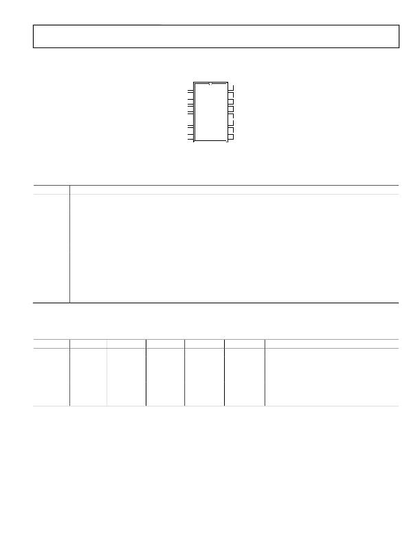
PIN CONFIGURATION AND FUNCTION DESCRIPTIONS
ADuM6132
V DD 1
GND 2
16 V ISO
15 GND ISO
V DDL 3
V IA 4
V IB 5
V OB 6
V DDB 7
ADuM6132
TOP VIEW
(Not to Scale)
14 GND A
13 V DDA
12 V OA
11 NC
10 NC
GND 8
9
GND ISO
NC = NO CONNECT
Figure 3. Pin Configuration
Table 8. Pin Function Descriptions
Pin No.
1
2, 8
3
4
5
6
7
9, 15
10, 11
12
13
14
16
Mnemonic
V DD
GND
V DDL
V IA
V IB
V OB
V DDB
GND ISO
NC
V OA
V DDA
GND A
V ISO
Description
Input Supply Voltage for Isolated Power Supply, 4.5 V to 5.5 V.
Ground Reference for Isolated Power Supply Input and Logic Inputs.
Input Supply Voltage for Logic, 4.5 V to 5.5 V.
Logic Input A.
Logic Input B.
Output B (Nonisolated).
Output B Supply Voltage Input (Nonisolated), 12.5 V to 17 V.
Ground Reference for Isolated Power Supply Output.
No Connect.
Output A (Isolated).
Output A Supply Voltage Input. Must be connected externally to V ISO (Pin 16).
Output A Ground Reference. Must be connected externally to GND ISO (Pin 15).
Isolated Power Supply Voltage Output.
Table 9. Truth Table (Positive Logic) 1
V IA Input
L
L
H
H
X
V IB Input
L
H
L
H
X
V DDL State
Powered
Powered
Powered
Powered
Unpowered
V DDB State
Powered
Powered
Powered
Powered
Powered
V OA Output
L
L
H
H
L
V OB Output
L
H
L
H
L
Notes
V OA returns to input state within 1 μs of V DDL
power restoration
X
X
Powered
Unpowered
L
L
1
L = low; H = high; X = high or low.
Rev. B | Page 7 of 16
发布紧急采购,3分钟左右您将得到回复。
相关PDF资料
ADUM6201CRIZ
ISOLATED DC-DC CONV 2CH 16SOIC
ADUM6404ARWZ
IC ISOLATOR 4CH DCDC CONV 16SOIC
ADUM7241CRZ-RL7
ISOLATOR DGTL 1KVRMS 2CH 8SOIC
ADUM7440CRQZ-RL7
IC DIGITAL ISOLATOR 4CH 16QSOP
ADUM7510BRQZ
IC DGTL ISOLATOR 5CH 16QSOP
ADZS-21364-EZLITE
KIT EVAL EZ LITE ADDS-21364
ADZS-21371-EZLITE
KIT EVAL EZLITE ADZS-21371
ADZS-21469-EZLITE
KIT EVAL EZ LITE ADSP-21469
相关代理商/技术参数
ADUM6200
制造商:AD 制造商全称:Analog Devices 功能描述:Dual-Channel, 5 kV Isolators with Integrated DC-to-DC Converter
ADUM6200ARIZ
功能描述:IC ISOLATOR DGTL 2CH 16SOIC RoHS:是 类别:隔离器 >> 数字隔离器 系列:IsoPower®, iCoupler® 产品培训模块:IsoLoop® Isolator 标准包装:50 系列:IsoLoop® 输入 - 1 侧/2 侧:5/0 通道数:5 电源电压:3 V ~ 5.5 V 电压 - 隔离:2500Vrms 数据速率:110Mbps 传输延迟:12ns 输出类型:CMOS 封装/外壳:16-SOIC(0.154",3.90mm 宽) 供应商设备封装:16-SOIC N 包装:管件 工作温度:-40°C ~ 85°C 其它名称:390-1053-5
ADUM6200ARIZ-RL
功能描述:IC ISOLATOR DGTL 2CH 16SOIC RoHS:是 类别:隔离器 >> 数字隔离器 系列:IsoPower®, iCoupler® 产品培训模块:IsoLoop® Isolator 标准包装:50 系列:IsoLoop® 输入 - 1 侧/2 侧:5/0 通道数:5 电源电压:3 V ~ 5.5 V 电压 - 隔离:2500Vrms 数据速率:110Mbps 传输延迟:12ns 输出类型:CMOS 封装/外壳:16-SOIC(0.154",3.90mm 宽) 供应商设备封装:16-SOIC N 包装:管件 工作温度:-40°C ~ 85°C 其它名称:390-1053-5
ADUM6200ARWZ
功能描述:ISOLAT DGTL 5KVRMS 2CH 16SOIC-W RoHS:是 类别:隔离器 >> 数字隔离器 系列:IsoPower®, iCoupler® 产品培训模块:IsoLoop® Isolator 标准包装:50 系列:IsoLoop® 输入 - 1 侧/2 侧:5/0 通道数:5 电源电压:3 V ~ 5.5 V 电压 - 隔离:2500Vrms 数据速率:110Mbps 传输延迟:12ns 输出类型:CMOS 封装/外壳:16-SOIC(0.154",3.90mm 宽) 供应商设备封装:16-SOIC N 包装:管件 工作温度:-40°C ~ 85°C 其它名称:390-1053-5
ADUM6200ARWZ-RL
功能描述:隔离器接口集成电路 kV 2-Ch Isolator w/ Int DC/DC Converter RoHS:否 制造商:Texas Instruments 通道数量:2 传播延迟时间: 电源电压-最大:5.5 V 电源电压-最小:3 V 电源电流:3.6 mA 功率耗散: 最大工作温度:+ 125 C 安装风格: 封装 / 箱体:SOIC-8 封装:Tube
ADUM6200CRIZ
功能描述:ISOLATED DC-DC CONV 2CH 16SOIC RoHS:是 类别:隔离器 >> 数字隔离器 系列:IsoPower®, iCoupler® 产品培训模块:IsoLoop® Isolator 标准包装:50 系列:IsoLoop® 输入 - 1 侧/2 侧:5/0 通道数:5 电源电压:3 V ~ 5.5 V 电压 - 隔离:2500Vrms 数据速率:110Mbps 传输延迟:12ns 输出类型:CMOS 封装/外壳:16-SOIC(0.154",3.90mm 宽) 供应商设备封装:16-SOIC N 包装:管件 工作温度:-40°C ~ 85°C 其它名称:390-1053-5
ADUM6200CRIZ-RL
功能描述:IC ISOLATOR DGTL 2CH 16SOIC RoHS:是 类别:隔离器 >> 数字隔离器 系列:IsoPower®, iCoupler® 产品培训模块:IsoLoop® Isolator 标准包装:50 系列:IsoLoop® 输入 - 1 侧/2 侧:5/0 通道数:5 电源电压:3 V ~ 5.5 V 电压 - 隔离:2500Vrms 数据速率:110Mbps 传输延迟:12ns 输出类型:CMOS 封装/外壳:16-SOIC(0.154",3.90mm 宽) 供应商设备封装:16-SOIC N 包装:管件 工作温度:-40°C ~ 85°C 其它名称:390-1053-5
ADUM6200CRWZ
功能描述:ISOLAT DGTL 5KVRMS 2CH 16SOIC-W RoHS:是 类别:隔离器 >> 数字隔离器 系列:IsoPower®, iCoupler® 产品培训模块:IsoLoop® Isolator 标准包装:50 系列:IsoLoop® 输入 - 1 侧/2 侧:5/0 通道数:5 电源电压:3 V ~ 5.5 V 电压 - 隔离:2500Vrms 数据速率:110Mbps 传输延迟:12ns 输出类型:CMOS 封装/外壳:16-SOIC(0.154",3.90mm 宽) 供应商设备封装:16-SOIC N 包装:管件 工作温度:-40°C ~ 85°C 其它名称:390-1053-5
